Breaking barriers to quantum sensing for civil, defense and intel
Leidos works on accelerating quantum technologies for missions, using photonic integrated circuits to tackle key challenges to deployment and integration at scale
Three Points to Remember
- The current optical, cooling and power equipment needed to perform quantum sensing, which is more capable and resistant to errors than classical sensors, can occupy an entire room, hampering usability in the field.
- Photonic integrated circuits, a microchip form of technology, can miniaturize optical functions and drastically reduce power and cooling needs, potentially enabling integration of quantum sensor setups into mission platforms.
- Leidos is driving photonic chip development in parallel with designing and building quantum sensors for potential applications in navigation, structural analysis and space observation.
Quantum sensing uses atomic-scale phenomena that enable extremely precise measurement of physical signals and properties. It can potentially redefine how civil, defense and other missions see and analyze their operational environments and conditions, if we can overcome currently restrictive hardware size, weight and power (SWaP) as well as noise challenges.
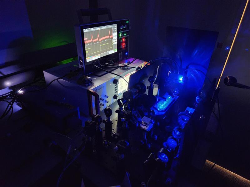
Leidos is on multiple development paths to field devices integrating both sensors and photonics (a branch of optics) that can work with quantum interactions in light and matter particles. The biggest of these paths is literally the smallest: photonic integrated circuits, or PICs.
“Our focus is near-term fieldable devices that can operate at room temperatures, are resilient to noise and have small form factors,” said Ben McDowell, quantum material scientist and device simulation lead at Leidos. “The integrated photonics we’re developing is fundamental to doing quantum sensing practically.”
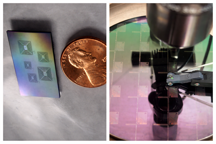
Photonic integrated circuits: thumbnail-sized optics
“Quantum sensing can detect what classical sensors can’t, or it can sense the same things with higher sensitivity or bandwidth,” McDowell continued. But, he noted, present equipment setups “can fill the back of a U-Haul truck with their huge free-space optics.”
It’s why most quantum sensing setups are currently confined to lab environments. But PICs, a growing technology, can pack many optical components into a microchip and make it possible to take quantum sensing onto mission platforms.
Whereas conventional optical systems use lenses and mirrors, PICs use micron-scale integrated circuit components to control light and enable the quantum information that's encoded within it to be generated, transmitted and processed.
“It’s many of the things found in the lab,” McDowell explained of the optical functions being shrunk into the photonic chips. “Some are more difficult to integrate than others, but the general idea is that for each free-space component, there’s an analogous chip-based component.”

Quantum sensing can detect what classical sensors can’t, or it can sense the same things with higher sensitivity or bandwidth. The integrated photonics we’re developing is fundamental to doing quantum sensing practically.
Ben McDowell
Leidos Quantum Material Scientist and Device Simulation Lead
Unlike electrons that move inside normal integrated circuits, photons have neither mass nor inertia. They also don’t experience resistance with the materials they travel through in the way electrons do. PICs, therefore, require significantly less cooling and power due to the lack of heat-generating resistance.
The high thermal stability of photons also means that cryogenic cooling isn’t needed for PIC-based systems. Many other quantum systems need to be at near-absolute-zero temperatures to tamp down thermal energy that destabilizes delicate quantum phenomena.
Photonic chips work at room temperatures and contribute to the ability to downsize hardware and equipment. PICs have additional advantages, including being easier to rapid prototype, scale up and integrate with other electronics in mission systems.
“Integrated photonics is a way of approaching everything that isn’t going to be fieldable and making chip-sized quantum devices without cryogenics,” said Brad Moores, quantum solution architect at Leidos who’s leading the development of PIC-based solutions.

Integrated photonics is a way of approaching everything that isn’t going to be fieldable. We are trying to get to the point where what we’re developing is close to what our customers want and we can adapt to their needs quickly.
Brad Moores
Leidos Quantum Solution Architect
Designed in house and sent to commercial semiconductor foundries for fabrication, the PICs are packaged with quantum sensors, lasers, power sources, photon detectors and electronics for signal processing.
Miniaturized sensing device packages would fit onto drones, small space payloads and other platforms where room is limited. Work is underway to possibly add detectors and embedded processing onto the PICs to reduce signal latency and loss while lowering SWaP even further.
Where can quantum sensing be used?
Sensing of quantum characteristics can detect physical properties, measure small changes and expose details beyond conventional sensors, especially with electric, magnetic and gravitational fields. In airborne navigation, Leidos is supporting the Defense Innovation Unit (DIU) and its Transition of Quantum Sensing (TQS) program on development of a sensor that would enable navigation via the Earth’s magnetic signals.
In gravity imaging, or gravimetry, quantum sensing could look at the conditions of infrastructure beneath surfaces with ranges in the tens of meters, surpassing those of classical gravimeters. One potential application is assessing the foundations of bridge piers supporting our roads and highways.

Quantum gravimetry scans the local gravitational field and produces matter-wave interference patterns. Since gravity penetrates all matter, the density variations in subsurface bulk masses show up as specific pattern signatures, which can support the measurement of groundwater movement, soil erosion and material deterioration.
“Quantum gravimetry lets us assess things we aren’t able to do with current state of the art,” McDowell said.
The technology can potentially expand automated inspection capabilities.
“It would add to what Leidos already does with drone-based lidar inspection of infrastructure,” he noted, referring to the use of light detection and ranging for above-ground assessments.
Quantum gravimetry involves trapping a cloud of atoms, cooling them to near-absolute-zero temperatures using lasers and dropping them into free fall, where their quantum effects can be used to perform measurements.
At the moment, the large SWaP of free-space optical traps limits cold-atom devices from being used in the field. A chip-based atom trap would bring about a 50-times SWaP reduction compared to classical optics setups that can take up entire large tabletops. Leidos is aiming to have a working prototype within two years.
Leidos is also working on quantum sensing of radio signals in space. Conventional radio frequency (RF) satellite antennas can span several meters in diameter. Plus, different antennas are needed to scan specific frequency bands across the RF spectrum.
The PIC-based device being developed would have low SWaP and wide bandwidth, detecting gigahertz and terahertz signals with a single unit.
In quantum RF sensing, lasers are used to energize neutral atoms to become sensitive to electric fields. The excited particles, called Rydberg atoms, essentially become the antenna, and exciting them to different energy levels enables the sensor to switch across a wide bandwidth of frequencies.
With a basic prototype planned for the end of this year, the quantum RF sensing package is envisioned to be the size of a printed circuit board – conducive to scientific and national security mission concepts that intend to use constellations or swarms of nanosatellites just several cubic feet big and weighing only a few kilograms.
“To measure gigahertz frequencies, it’s really hard to fit a classical sensor into a CubeSat,” Moores said. “The quantum RF sensor we’re working on is a broadband device that has very sensitive field detection where you can change the frequency you’re measuring.”
Cutting the noise around quantum sensing
Smaller footprints mean much greater immunity from unwanted outside factors, as well. Component packages with large surface areas are more prone to thermal gradients around them and to vibrations that can lead to misalignments.
Then, there’s electromagnetic interference (EMI) from mission platforms and operational environments, such as aircraft cabins where the quantum sensor being developed in the TQS program would be used.
“There’s a tradeoff between having an incredibly sensitive sensor and putting it on a very noisy platform,” said Elizabeth Iwasawa, Leidos' director of quantum technologies. From a design and engineering standpoint, “you have this tension between it being useful and detrimental, so how do we make these sensors functional in the field?” she said.
“We know that quantum sensors have extremely high sensitivities and are very good in the lab, but as soon as you take them into the field, that sensitivity is a double-edged sword," Moores added.
Using light instead of electrons, PICs are inherently resilient to EMI. It’s one more notch in their list of design and performance benefits.

The allure of chip-based quantum sensing is that you can do it with smaller footprints and greater sensitivities. Finding the right foundry partners is critical to our success, from materials to scalability.
Elizabeth Iwasawa
Leidos Director of Quantum Technologies
Although it is driving PIC development, Leidos is collaborating with the ecosystem of platform, payload and signal processing providers to ensure that quantum capabilities can be integrated into a variety of mission systems. In the TQS program, EMI filtration, involving software-based calibration techniques and algorithms, is being used to help mitigate platform effects, transient events and error sources.
More work needs to be done before quantum sensing is field-ready. What makes the technology compelling, though, is its naturally-occurring and time-stable nature that brings us closer to resolute and accurate measurement capabilities, unlike classical sensing devices that are susceptible to thermally and mechanically induced drift.
Leidos has chosen PICs as the path to accelerate the readiness of quantum sensing devices. Through continued hardware prototyping, test and validation, driven by diverse mission and technical expertise across the company, it intends to have solutions that are as operationally feasible as possible.
“We are trying to get to the point where what we’re developing is close to what our customers want and we can adapt to their needs quickly,” Moores said.